Modular Power Stress Systems

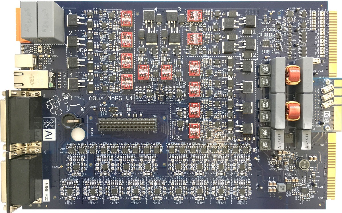
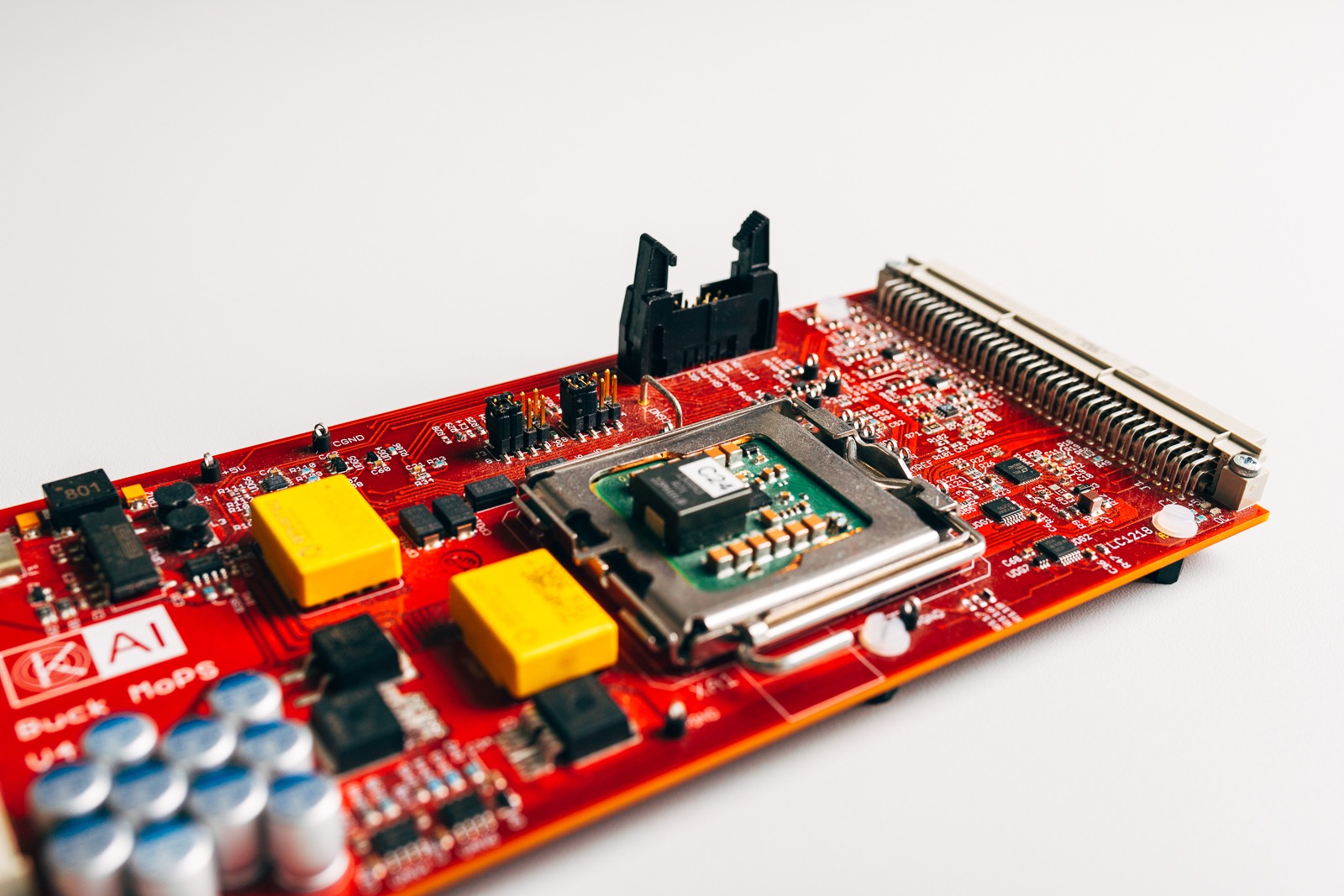
The modular power stress test system provides driving, protection, and diagnostic features for discrete and integrated power semiconductors during their initial design phase. This test concept allows the execution of flexible active power cycling stress tests based on test structures and engineering samples, even before the availability of final driver and protection circuits or dedicated application environments.
The modular concept provides an arbitrary, real-time controlled configuration of automated measurements and cyclic load sequences with preset voltage and/or current patterns over the whole power range required by the customer application. When reaching a previously defined electrical or thermal parameter deviation, components can be selectively disabled to retain them in a mostly unaltered state for further electrical and physical analysis.

A dedicated test system for testing of complex System-on-Chip products was implemented successfully within the Infineon reliability test environment. It enables comprehensive in-situ diagnosis and device data recording in real-time during the whole stress test. Also, next generation of Wide-Bandgap power semiconductors have been investigated extensively with test systems based on the modular power stress architecture.
The KAI laboratory test environment includes two high performance stress screening climate chambers with enhanced heating and cooling capability up to 8 K/min between -70 °C and +200 °C. Multiple high power DC supplies and active electronic loads ranging up to 2 kV / 100 A provide the power to verify the next generation of application module prototypes under variable environmental and electrical application conditions.


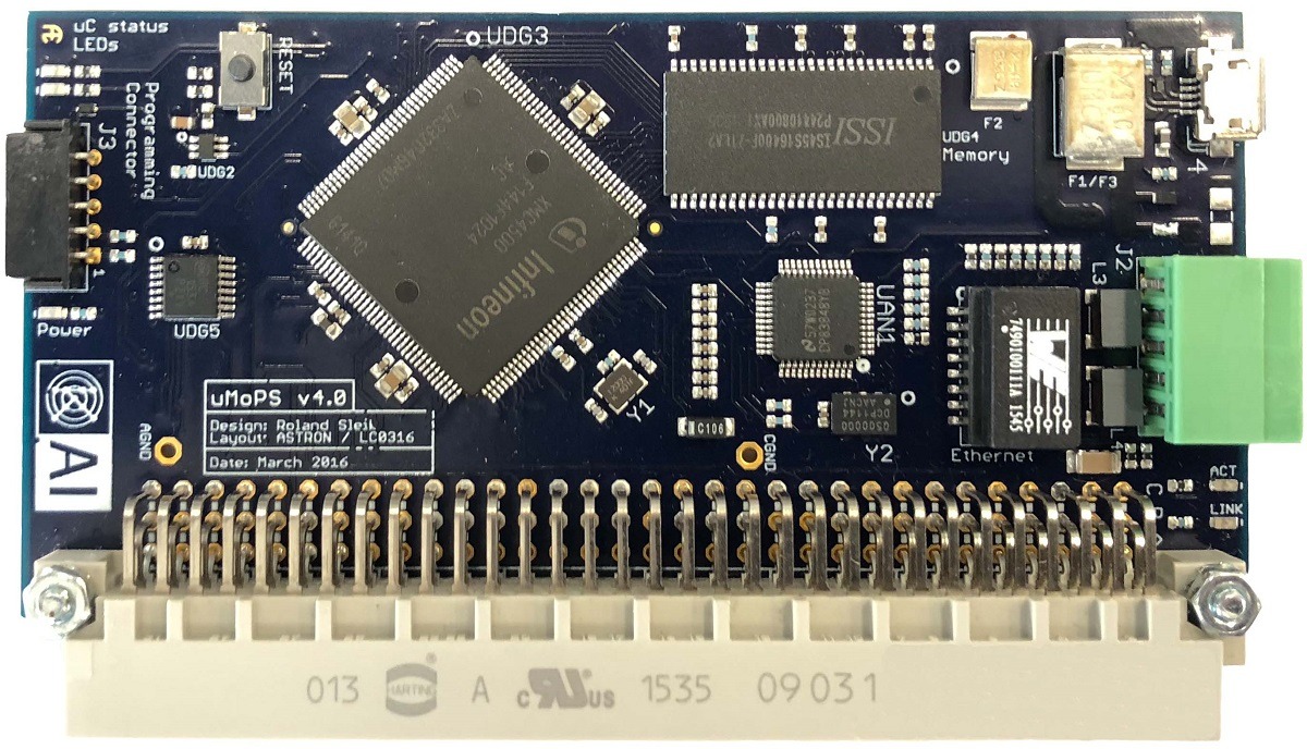
For applications in the climate chamber a dedicated test control and monitoring platform based on an automotive qualified 32-bit microcontroller has been developed. This modular test controller platform has been our workhorse for many years. As well as our test systems, the microcontroller is an in-house development and allows us to constantly improve and implement necessary new features for the evolving test requirements of next generation power semiconductors.
