Materials Science Laboratory
Scanning Electron Microscopy
Scanning electron microscopy (SEM) is a high-resolution characterization technique that probes a sample by scanning its surface with a focused electron beam. While scanning, the signals produced by the interaction of the electron beam with the sample are recorded with various detectors. The data is visualized in the form of an image of the scanned sample surface. Depending on the detector used, different properties can be primarily imaged, e.g. the sample’s surface topography or its composition. Advanced characterization techniques can be facilitated by equipping an SEM tool with additional detectors. For example, X-Ray Energy Dispersive Spectroscopy (XEDS) and Electron Backscatter Diffraction (EBSD) allow for characterization of the chemical composition of the sample and its microstructure, respectively. There are two SEM tools at KAI that serve as a means for characterization in different areas of research.
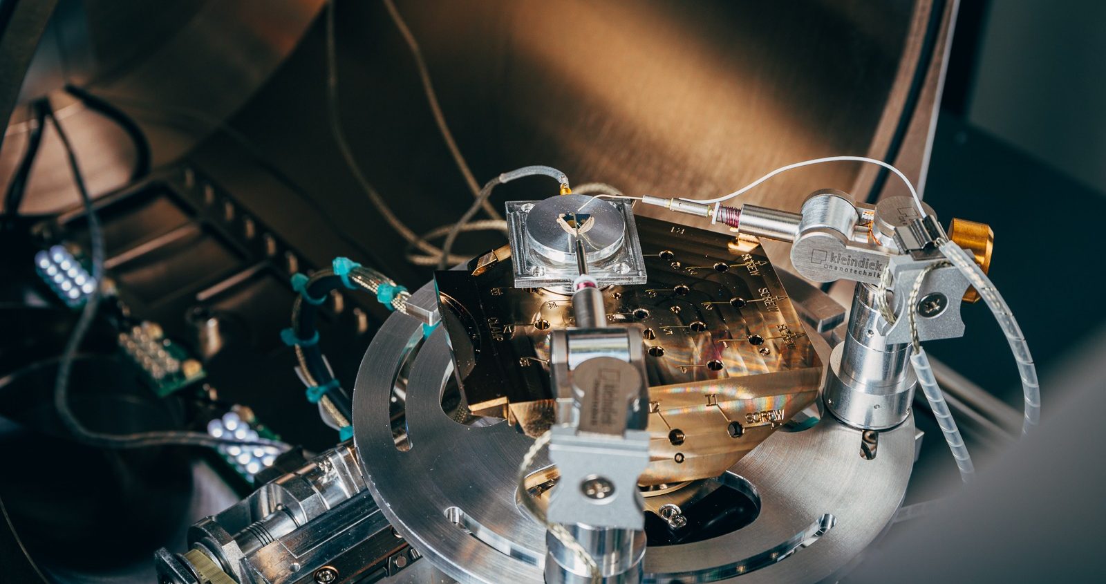
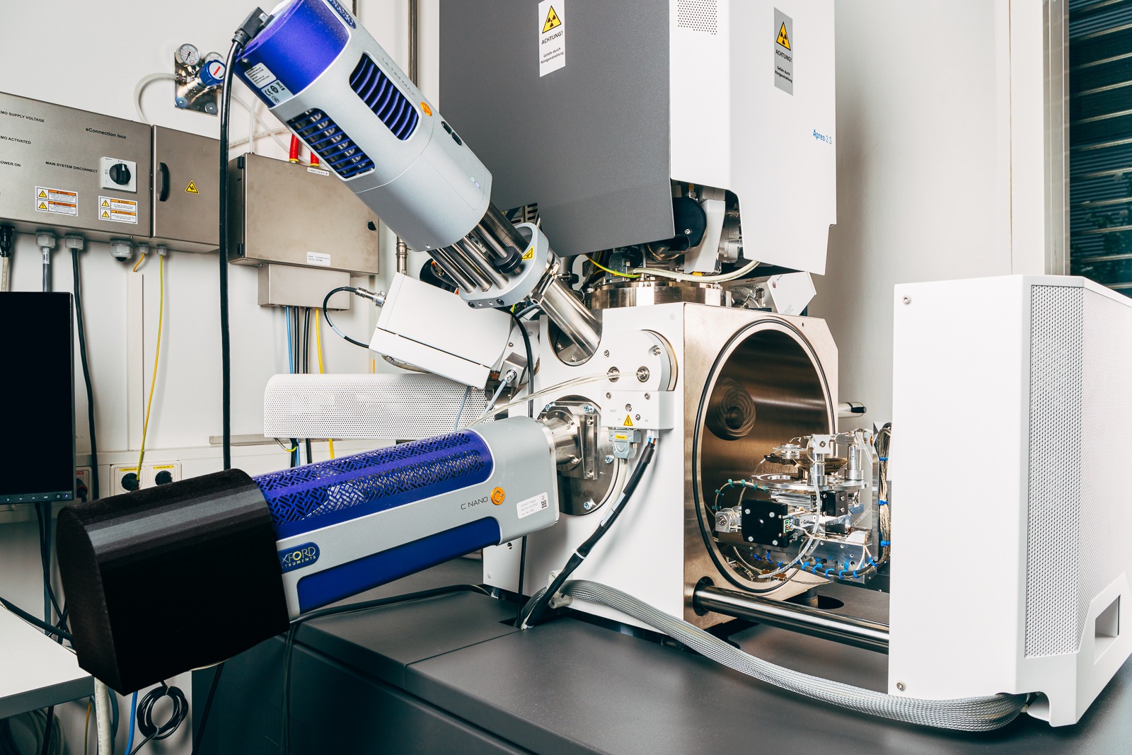
The Thermo Fisher Scientific Apreo 2 S HiVac is a versatile high-resolution SEM. It is equipped with an Everhart-Thornley detector, Trinity Detection System for simultaneous selective collection of backscattered/secondary/low-energy secondary electrons, an insertable segmented backscattered electron detector for energy filtered imaging and increased signal-to-noise, and XEDS and EBSD systems for chemical and microstructural characterization. The large specimen chamber, 1 nm resolution at 10 mm analytical working distance, and 105° stage tilt range allow for a wide range of sample geometries and in-situ experimental stages – such as a 3-probe Electron Beam Induced Current (EBIC) setup for defect analysis and resistance measurements in semiconductors and semiconductor devices, and a high-temperature heating stage for heating experiments and quantitative dopant contrast imaging in semiconductors. The Apreo 2 S is also equipped with a rocking-beam mode that, along with four other microscope modes, enables Electron Channeling Contrast Imaging (ECCI) for defect analyses in a range of materials from polycrystalline to magnetic single crystals.
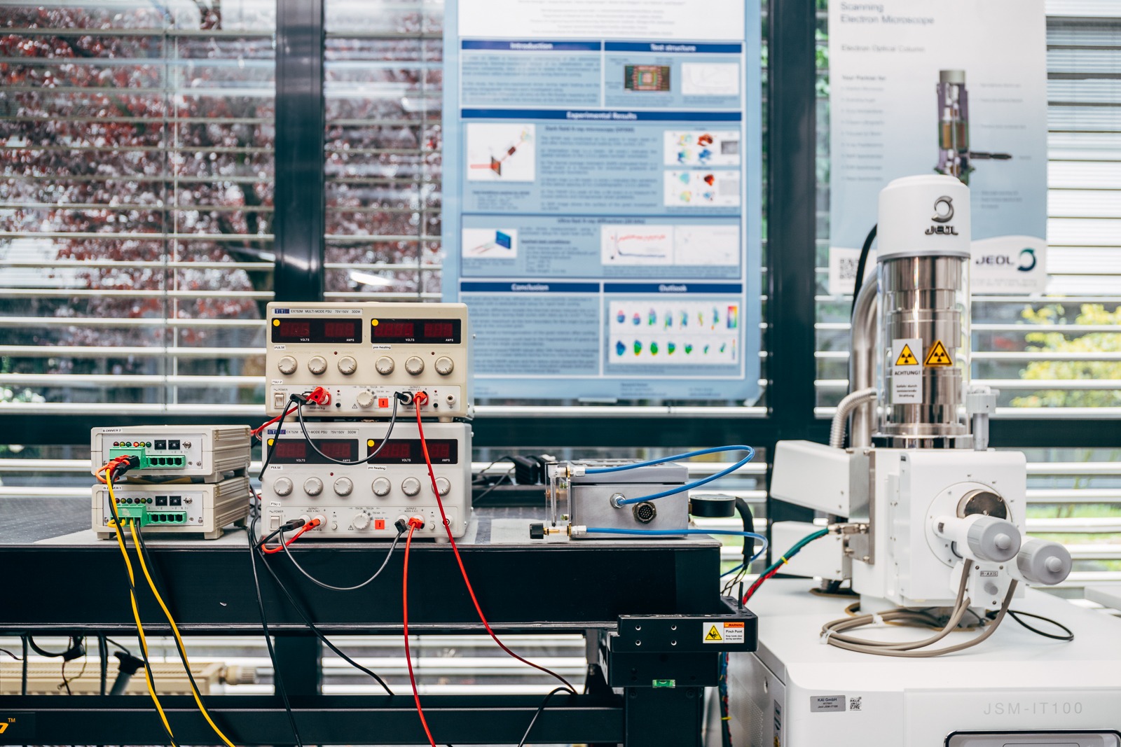
The second SEM tool at KAI, a JEOL JSM-IT100 InTouchScope™, is utilized in a more conventional sense of SEM. It is only equipped with a secondary electron detector and a backscatter electron detector. What makes this SEM tool unique though, is a cable feed-through to allow for electrically actuating microelectronic chips in situ. As an integral part of the “poly-heater experimental setup”, the JEOL JSM-IT100 is utilized to monitor progressing degradation of on-chip metallization layers during the course of thermo-mechanical fatigue tests.
Poly-heaters are special test chips that are provided with a resistive polycrystalline silicon layer (“poly”) with ohmic behavior, utilized for active heating. Within the materials science group at KAI, poly-heaters are employed as simplified test chips that can replicate the extreme thermal conditions occurring in smart power semiconductors during short-circuit or thermal overload events. By these means, the thermo-mechanical behavior of metallization layers can be investigated during the early development stages of future-generation chips.
The poly-heater experimental setup at KAI, with its in-house designed hard- and software, enables the execution of automated poly-heater fatigue tests. Such tests can optionally be accompanied by automated in-situ characterization, including electrical resistance measurements and/or SEM image acquisitions. With the capability to choose parameters pertaining to the thermal profile of the heat pulses applied for loading, highly comprehensive studies are possible.
Nanoindentation
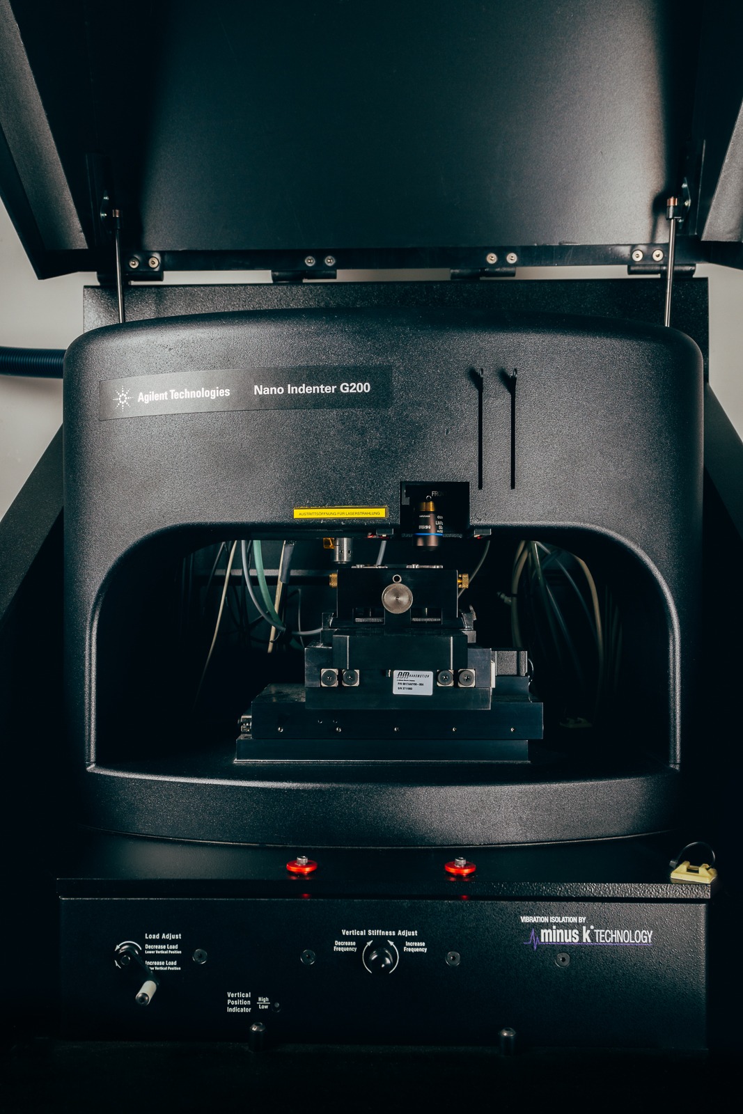
The method of nanoindentation is widely used to determine mechanical material properties such as hardness and Young’s modulus of materials. It can be used for thin films of less than 1 µm thickness to determine these values without the influence of the substrate material. During the measurement, a diamond tip of known shape is pressed into the sample with increasing force, with the tip displacement being continuously measured in parallel. From the resulting load-displacement-curve hardness and Young’s modulus can be calculated.
The Keysight G200 commercial nanoindenter located at KAI includes:
A heating option for temperature dependent measurements up to 500 °C in inert/active gas atmosphere.
A continuous stiffness measurement option for depth dependent material property measurement.
Express test parameter mapping for fast acquisition of material property maps.
Keysight NanoVision nanomechanical microscopy for specimen surface and indentation imprint imaging.
Besides standard nanoindentation measurements, methods to quantitatively measure coating adhesion, which have been developed in cooperation with academic partners, are in use at KAI.
Wafer Curvature
The wafer curvature technique is used to investigate the thermo-mechanical behavior of thin films on a substrate (a wafer) by monitoring its curvature while undergoing a thermal treatment. The measured curvature is related to the biaxial stress in the film, and from this, mechanical properties such as elastic modulus and temperature-dependent yield stress can be determined. Furthermore, processes such as recrystallization and stress relaxation can be captured.
The k-Space MOS Thermal Scan wafer curvature tool at KAI utilizes an optical module to measure curvature via an array of laser beams. By means of its rapid thermal processing system and its gas control units, the replication of relevant thermal treatments in terms of thermal profile and atmosphere is enabled. Temperatures are controlled precisely and may range from −55 °C (employing the optional feature of liquid-nitrogen cooling) to +600 °C.
Sample Preparation
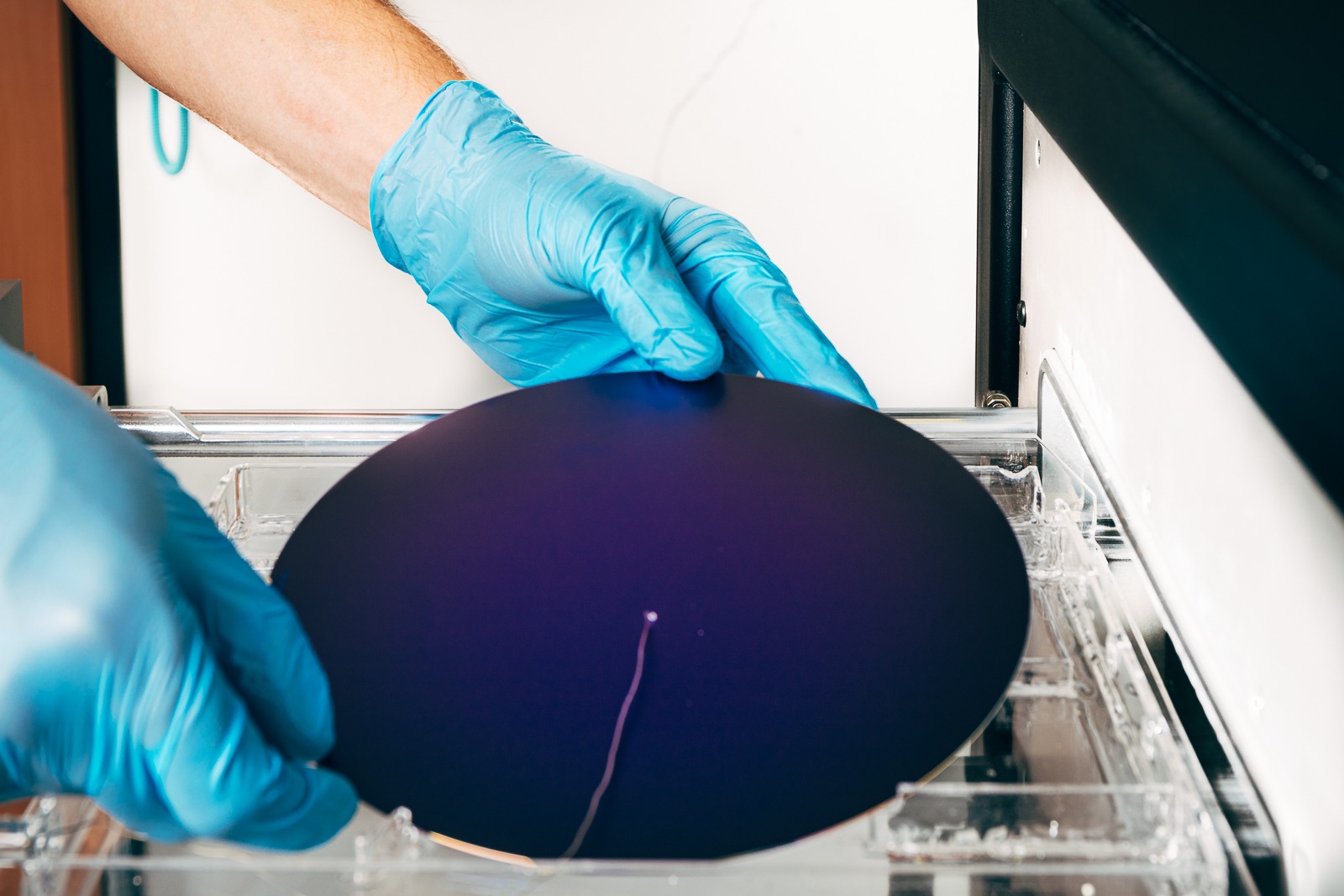
Samples that lie within the scope of interest at KAI – wafers, microelectronic chips, components, and modules – require a proper preparation for materials characterization. For example, it is required to cut a wafer into pieces to have samples that fit into the nanoindenter and a cross-sectional preparation of a chip is indispensable to investigate its layer stack by SEM. Multiple different tools are available at KAI, allowing successive sample preparation tasks from a rough to a fine level.
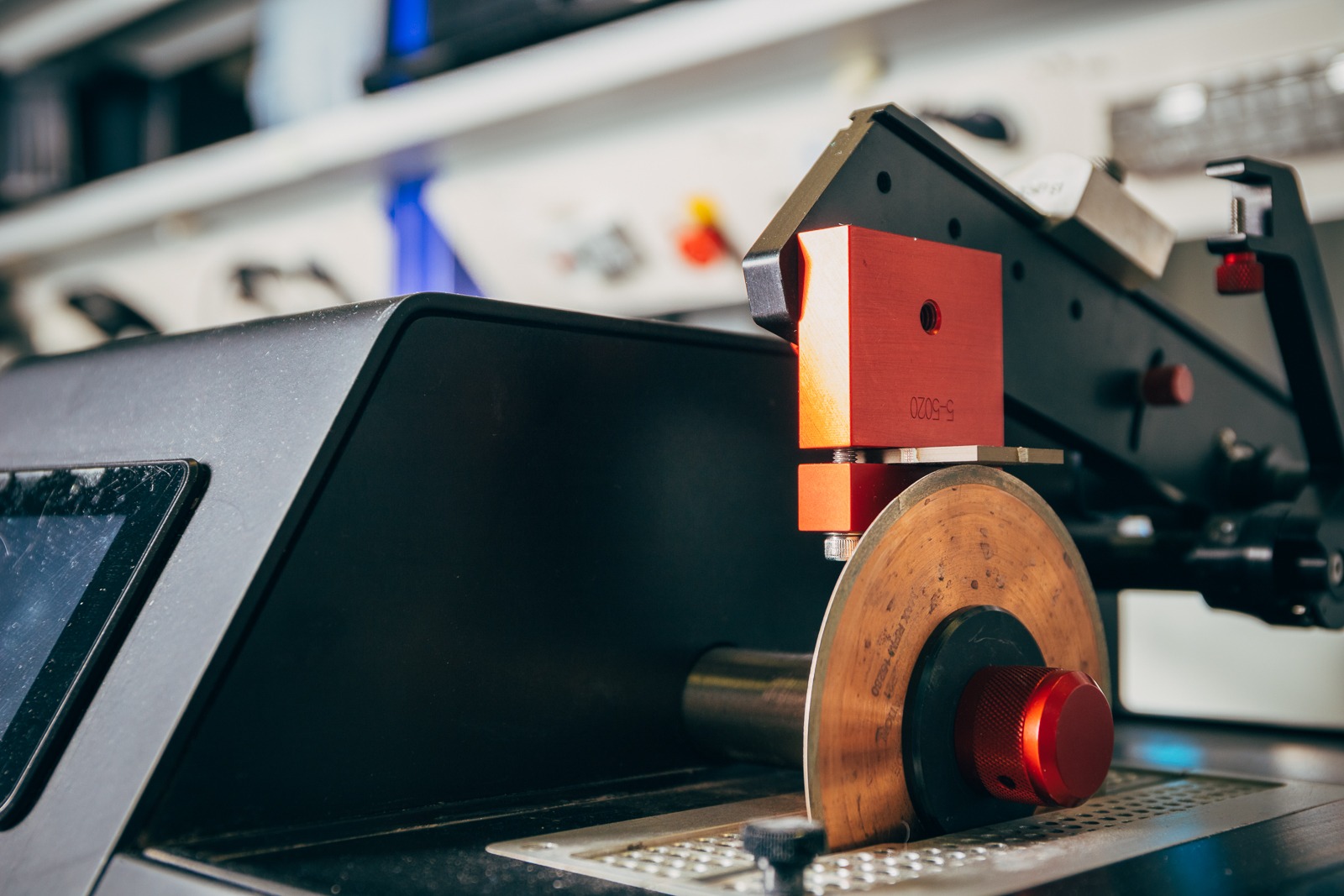
The Allied TechCut 4x™ Precision Low Speed Saw at KAI can be used for sawing wafer pieces, Printed Circuit Boards (PCBs), and packaged or embedded chips to prepare for further, more precise sample preparation tasks. It has a blade with a diamond abrasive material and a micrometer screw for precise alignment.
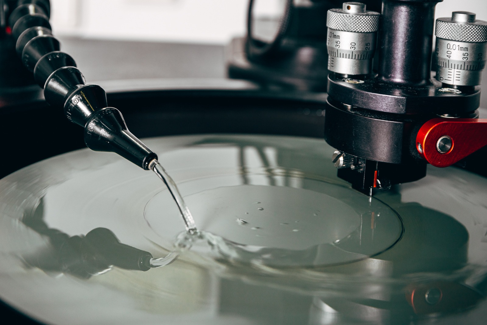
The Allied MultiPrep™ Precision Mechanical Polishing System can be used for grinding and polishing different sample types. It can be used with SiC and diamond polishing papers with a grit sizes between 30 µm and 0.1 µm as well as with different diamond suspensions. The material removal can be monitored to reach a target position of the sample. Both cross-sectional preparation as well as coplanar thinning is possible.
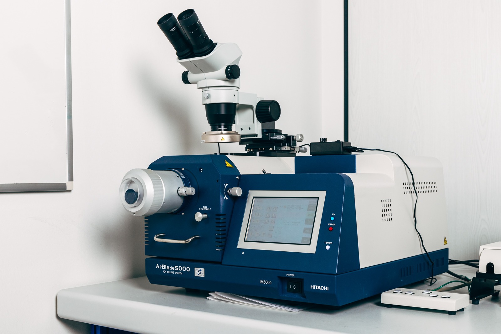
The Hitachi Ion Milling System ArBlade 5000 can be used to prepare samples by the irradiation of high-energy argon ions (2–8 kV). A flat milling mode and a cross-section milling mode, allow for targeted preparations with an accuracy of ≈10 µm. The resulting sample surface is free of mechanical deformation and contamination (e.g., abrasive grits, mud), which makes this preparation method especially appealing for subsequent characterization by SEM.
