Data Analytics & Data Science
The complexity of data generated by semiconductor industry demands for advanced analysis methods to support decision making processes.
The amount of data generated during the semiconductor development and manufacturing process and the subsequent verification and reliability analyses is large due to the high complexity of the products, but also diverse because the data sources include electrical and physical measurements, output from different type of sensors and images from physical failure inspection. Combining these data sources and extracting necessary information for decision making processes are important steps towards the digitalization of semiconductor industry. Data analytics and Data Science methods are powerful tools for the mentioned challenges, because they are able to consider large amounts of data and at the same time they can handle complex dependencies between data.

KAI Competences
The KAI Data Science group develops and applies data analysis concepts, advanced statistical methods and machine learning & deep learning algorithms for the semiconductor industry since 2013. In this time, we established key competences in the following areas:
- Statistical methods for lifetime and degradation modeling of semiconductor devices
- Methods for advanced statistical device screening and pattern recognition to identify risk devices in the electrical measurements after the semiconductor frontend production
- Computer vision for automatic extraction and quantification of visual information and for automated image classification
- Mathematical methods to develop dispatching and scheduling routines to optimize tool usage and resource planning in semiconductor labs
- ML methods for time series data to support decision making in the verification process
- Data pre-processing and data labelling methods for diverse data analysis and data science methods
- Development and maintenance of ML Pipelines (MLOps) for industrial use cases
Research Goals
The focus areas of the KAI Data Science group are:
- Robust estimation methods for non-linear models with non-standard data distributions
- Model deployment and frameworks for non-data scientist to train ML/DL models
- Classical computer vision methods to enable efficient and objective extraction of quantitative information out of images
- CNNs to automate image classification
- Development of highly-automated routines for ML/DL model maintenance to identify data-drift and concept drift (e.g. open set recognition methods, continual learning, self-supervised learning)
- Application of scheduling and (partial-)rescheduling routines, incl. the development of heuristics.
- ML/DL methods for time series analysis and classification
Data Analytics & Data Science Activities
Lifetime & Degradation Modelling
The reliability of modern power semiconductor devices is subject to strict requirements. In accelerated end-of-life tests, the robustness of the devices against externally applied stress is extensively tested, with the aim to predict the Safe Operating Area (SOA), illustrated in Figure 1, for different load conditions.
Since 2007, KAI is developing statistical lifetime and degradation models for power semiconductors in close cooperation with the process- and design engineers from Infineon Technologies and academic partners at renowned universities. The developed models provide a solid statistical framework to predict the lifetime. These models are used to accompany decisions during product development and at product qualification.
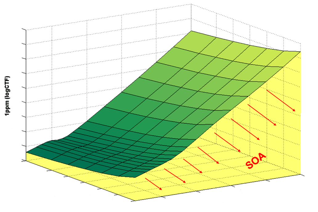
Figure 1: Schematic representation of the output from a statistical model to predict the safe operating area of a semiconductor device
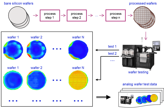
Figure 2: Schematic of the wafer test that depicts how wafer maps and analog wafer test data are generated.
Identification of patterns in analog wafer test data (electrical test)
The semiconductor manufacturing process comprises many stages to ensure the quality of produced semiconductor devices. One of these stages is called the wafer test (depicted in Figure 2), where the functionality of devices is tested and countermeasures are performed if deemed necessary, i.e. in case of process deviations.
A common way to detect these deviations during wafer test is the detection of so-called critical process patterns on the visualized test values (referred to as wafer maps). Typically, these patterns are pre- defined, salient structures that are visible on the wafer maps and deemed critical by domain experts.
At KAI we developed the Wafer Health Factor (WHF), a Machine Learning framework that is capable of automatically detecting critical process patterns in analog wafer test data, thus reducing considerably the manual inspection of wafer maps (as shown in Figure 3).
Beyond that, additional in-house applications are currently in development to further improve the benefit enabled by WHF, including
- the WHF Analysis Web App, an easy-to-use web application for product engineers to apply the WHF to their analog wafer test data,
- the WHF Monitoring Service, an automated inference framework that notifies product engineers in case critical process patterns are detected in nearly real-time,
- the WHF Model Monitoring framework that utilizes concept from Continual Learning to ensure constant and good model performances throughout a model’s lifetime.
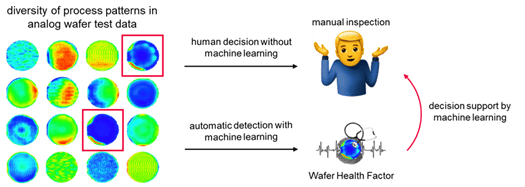
Figure 3: Workflow of how to automatically detect critical process patterns in analog wafer test data by using a machine learning application.
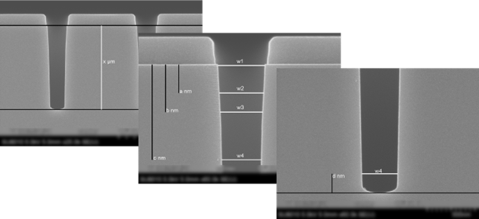
Figure 4: Automated trench measurements in SEM images
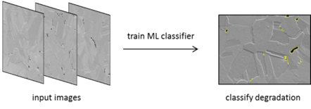
Figure 5: Automatic classification of degradation features in metal layers.
Automatic extraction and quantification of visual information
During development and production of semiconductor devices, many visual inspections are performed. The information in the images is used for development decisions or to control the production process. To this end, quantitative information needs to be extracted.
For highly repetitive tasks (e.g. trench measurements) or tasks that are difficult for humans (e.g. identification of all damage features in one image), Computer Vision methods can be used. At KAI we develop classical Computer Vision algorithms to automatically
- Calibrate and pre-process images
- Segment and measure features in images
- Classify degradation features in metal layers
- Identify microstructures of metal layers
Automatic image classification
Automatic classification of defect images in production environments is becoming increasingly important. It has a positive effect on the efficiency of the workflow and provides objective and reproducible classification results. Therefore, the aim of these activities is to replace the state-of-the-art manual classification of defect density SEM images i semiconductor fabs by an automatic image classification pipeline. The heart of this pipeline is a conventional CNN architecture, initialized with the ImageNet weights and retrained and fine-tuned on our defect density SEM images. Overall, the pipeline development focuses on
- generalization of the model
- development of model monitoring concepts
- development of open-set recognition methods to identify new defect classes
- increase the automation degree of the classification pipeline
Here you find more information.
Scheduling and Dispatching
In the intricate world of semiconductor manufacturing, precision and efficiency take central stage. This field is characterized by a multitude of intricate processing steps requiring exceptional expertise and advanced technological tools. Behind the scenes is a meticulously orchestrated interplay of processes and equipment guided by careful planning approaches. The aim is to explore the centrality of mathematical scheduling and dispatching in semiconductor laboratories using careful strategic planning and fine-tuned optimization finally leading to improved resource utilization and efficiency.
Precisely, KAI is focusing on
- data and process mining algorithms to generate viable and reliable scheduling instances,
- a stepwise data quality improvement in the relevant domains,
- the development of automated scheduling and dispatching solutions,
- event- and deviation-driven (partial-) rescheduling techniques in order to react on disruptions dynamically.
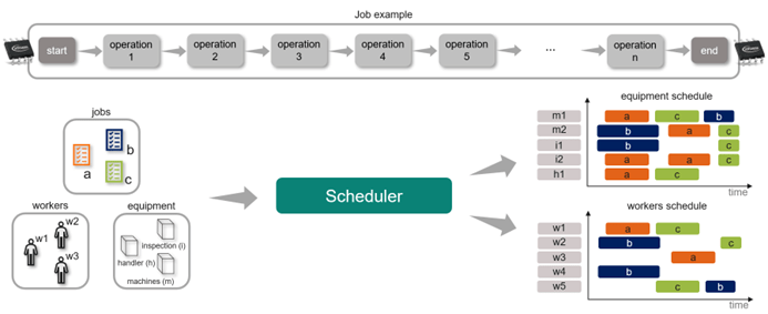
Figure 6: Schematic representation of optimized scheduling.
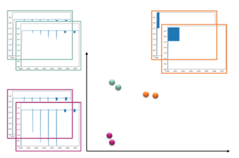
Figure 7: Schematic representation of a waveform clustering algorithm.
Time series clustering and anomaly detection
The post-silicon verification process of semiconductor devices takes place on actual devices and includes the analysis of a large amount of time series data. These data sets are generated by varying the input parameters and measuring the response of the device. Manual visual inspection is often not economically feasible, therefore algorithms to identify suspicious data series are needed.
In this project, KAI focuses on the
- Evaluation of waveform clustering algorithms and tools to identify suspicious data series in post-silicon verification data
- Development of methods to automate data pre-processing in Infineon verification labs
- Development of a standardized data pipeline
- Evaluation of Design of Experiment (DoE) algorithms and tools to optimize the amount of verification tests
